本帖最后由 埃律西昂 于 2022-6-30 22:40 编辑
来源:Anandtech
原英文标题:《As HPC Chip Sizes Grow, So Does the Need For 1kW+ Chip Cooling》

One trend in the high performance computing (HPC) space that is becoming increasingly clear is that power consumption per chip and per rack unit is not going to stop with the limits of air cooling. As supercomputers and other high performance systems have already hit – and in some cases exceeded these limits – power requirements and power densities have continued to scale up. And based on the news from TSMC's recent annual technology symposium, we should expect to see this trend continue as TSMC lays the groundwork for even denser chip configurations.
高性能计算(HPC)领域越来越清晰的一个趋势是,每个芯片和每个机架单元的功耗不会随着空气冷却的限制而停止。随着超级计算机和其他高性能系统已经达到并在某些情况下超过了这些限制,功率要求和功率密度继续扩大。根据台积电最近年度技术研讨会的消息,我们应该期待看到这一趋势继续下去,因为台积电为更密集的芯片配置奠定了基础。
The problem at hand is not a new one: transistor power consumption isn't scaling down nearly as quickly as transistor sizes. And as chipmakers are not about to leave performance on the table (and fail to deliver semi-annual increases for their customers), in the HPC space power per transistor is quickly growing. As an additional wrinkle, chiplets are paving the way towards constructing chips with even more silicon than traditional reticle limits, which is good for performance and latency, but even more problematic for cooling.
手头的问题并不新鲜:晶体管功耗的缩小速度并不像晶体管尺寸那样快。由于芯片制造商不会将性能放在桌面上(并且无法为其客户提供半年一年的增长),因此在HPC空间中,每个晶体管的功率正在快速增长。作为额外的褶皱,小芯片正在为构建比传统光罩限制更多的硅的芯片铺平道路,这对性能和延迟有好处,但对冷却来说更成问题。
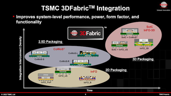
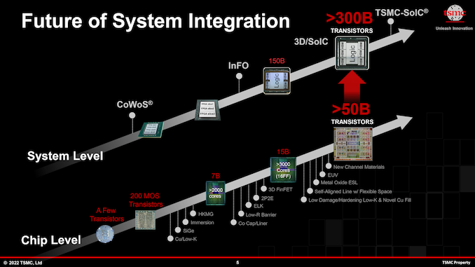
Enabling this kind of silicon and power growth has been modern technologies like TSMC'a CoWoS and InFO, which allow chipmakers to build integrated multi-chiplet system-in-packages (SiPs) with as much a double the amount of silicon otherwise allowed by TSMC's reticle limits. By 2024, advancements of TSMC's CoWoS packaging technology will enable building even larger multi-chiplet SiPs, with TSMC anticipating stitching together upwards of four reticle-sized chiplets, This will enable tremendous levels of complexity (over 300 billion transistor per SiP is a possibility that TSMC and its partners are looking at) and performance, but naturally at the cost of formidable power consumption and heat generation.
实现这种硅和功率增长的是台积电CoWoS和InFO等现代技术,这些技术允许芯片制造商构建集成的多芯片系统级封装(SiP),其硅量是台积电光罩限制所允许的两倍。到2024年,台积电CoWoS封装技术的进步将能够构建更大的多芯片系统级封装,台积电预计将拼接在一起超过四个光罩大小的小芯片,这将实现巨大的复杂性(台积电及其合作伙伴正在考虑的每个SiP超过3000亿个晶体管)和性能,但自然会以巨大的功耗和发热为代价。

Already, flagship products like NVIDIA's H100 accelerator module require upwards of 700W of power for peak performance. So the prospect of multiple, GH100-sized chiplets on a single product is raising eyebrows – and power budgets. TSMC envisions that several years down the road there will be multi-chiplet SiPs with a power consumption of around 1000W or even higher, Creating a cooling challenge.
像 NVIDIA 的 H100 加速器模块这样的旗舰产品已经需要高达 700W 的功率才能达到峰值性能。因此,在单个产品上使用多个GH100尺寸的小芯片的前景正在引起人们的注意 - 以及功率预算。台积电设想,几年后将出现功耗约为1000W甚至更高的多芯片系统级封装,这带来了冷却挑战。
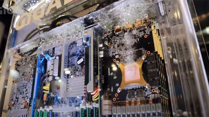
At 700W, H100 already requires liquid cooling; and the story is much the same for the chiplet based Ponte Vecchio from Intel, and AMD's Instinct MI250X. But even traditional liquid cooling has its limits. By the time chips reach a cumulative 1 kW, TSMC envisions that datacenters will need to use immersion liquid cooling systems for such extreme AI and HPC processors. Immersion liquid cooling, in turn, will require rearchitecting datacenters themselves, which will be a major change in design and a major challenge in continuity.
在700W时,H100已经需要液体冷却;对于英特尔的基于小芯片的Ponte Vecchio和AMD的Instinct MI250X来说,情况大致相同。但即使是传统的液体冷却也有其局限性。当芯片达到累计1千瓦时,台积电设想数据中心将需要使用浸入式液体冷却系统来应对这种极端的AI和HPC处理器。反过来,浸入式液体冷却将需要重新构建数据中心本身,这将是设计上的重大变化,也是连续性的主要挑战。
The short-tem challenges aside, once datacenters are setup for immersion liquid cooling, they will be ready for even hotter chips. Liquid immersion cooling has a lot of potential for handling large cooling loads, which is one reason why Intel is investing heavily in this technology in an attempt to make it more mainstream.
撇开短时间的挑战不谈,一旦数据中心设置为浸入式液体冷却,它们将准备好使用更热的芯片。液浸式冷却在处理大型冷却负载方面具有很大的潜力,这也是英特尔大力投资这项技术以使其更加主流的原因之一。

In addition to immersion liquid cooling, there is another technology that can be used to cool down ultra-hot chips — on-chip water cooling. Last year TSMC revealed that it had experimented with on-chip water cooling and said that even 2.6 kW SiPs could be cooled down using this technology. But of course, on-chip water cooling is an extremely expensive technology by itself, which will drive costs of those extreme AI and HPC solutions to unprecedented levels.
除了浸入式液体冷却外,还有另一种技术可用于冷却超热芯片 - 片上水冷却。去年,台积电透露,它已经对片上水冷却进行了实验,并表示使用该技术甚至可以冷却2.6 kW SiP。但是,当然,片上水冷却本身就是一项极其昂贵的技术,这将把这些极端人工智能和HPC解决方案的成本提高到前所未有的水平。
None the less, while the future isn't set in stone, seemingly it has been cast in silicon. TSMC's chipmaking clients have customers willing to pay a top dollar for those ultra-high-performance solutions (think operators of hyperscale cloud datacenters), even with the high costs and technical complexity that entails. Which to bring things back to where we started, is why TSMC has been developing CoWoS and InFO packaging processes on the first place – because there are customers ready and eager to break the reticle limit via chiplet technology. We're already seeing some of this today with products like Cerebras' massive Wafer Scale Engine processor, and via large chiplets, TSMC is preparing to make smaller (but still reticle-breaking) designs more accessible to their wider customer base.
尽管如此,虽然未来不是一成不变的,但它似乎已经铸在硅中。台积电的芯片制造客户愿意为这些超高性能解决方案(想想超大规模云数据中心的运营商)支付高价,即使成本和技术复杂性很高。要把事情带回我们开始的地方,就是台积电一开始就开发CoWoS和InFO封装工艺的原因——因为有客户准备并渴望通过小芯片技术打破光罩限制。我们今天已经看到像Cerebras的大规模晶圆级引擎处理器这样的产品,通过大型芯粒,台积电正准备让更小(但仍然破罩)的设计更容易被更广泛的客户群所接受。
Such extreme requirements for performance, packaging, and cooling not only push producers of semiconductors, servers, and cooling systems to their limits, but also require modifications of cloud datacenters. If indeed massive SiPs for AI and HPC workloads become widespread, cloud datacenters will be completely different in the coming years.
这种对性能、封装和冷却的极端要求不仅将半导体、服务器和冷却系统的生产商推向了极限,而且还需要对云数据中心进行修改。如果AI和HPC工作负载的大规模系统级封装确实变得普遍,那么未来几年云数据中心将完全不同。 |
 310112100042806
