本帖最后由 埃律西昂 于 2022-11-29 20:48 编辑

来源: 三星半导体
原英文标题:《A Bridge Between Worlds: How Samsung’s GDDR6W Creates Immersive Metaverse Experiences with Powerful Graphics Memory》
As advanced graphics and display technologies develop, they are blurring the lines between metaverse and our everyday experience. Much of this important shift is being made possible by the advancement of memory solutions designed for graphics products.
随着先进的图形和显示技术的发展,它们正在模糊元宇宙与我们的日常体验之间的界限。这一重要转变在很大程度上得益于为图形产品设计的内存解决方案的进步。
High-bandwidth Graphics Memory Solution: The Key to Hyper-real Gaming and Digital twin
高带宽显存解决方案:超真实游戏和数字孪生的关键
One of the biggest challenges for improving virtual reality is taking the complexities of real-world objects and environments and recreating them in a virtual space. Doing so requires massive memory and increased computing power. At the same time, the benefits of creating more true-to-life metaverse will be far reaching, including real-life simulations of complicated scenarios and more, sparking innovation across a number of industries.
改善虚拟现实的最大挑战之一是将现实世界对象和环境的复杂性在虚拟空间中重新创建。这样做需要大量内存和增强的计算能力。与此同时,创建更逼真的元宇宙的好处将是深远的,包括复杂场景的真实模拟等,激发多个行业的创新。
This is the central idea behind one of the most popular concepts in virtual reality: digital twin. A digital twin is a virtual representation of an object or space. Updated in real-time in accordance with the actual environment, a digital twin spans the lifecycle of its source and uses simulation, machine learning and reasoning to help decision-making. While until recently this was not feasible proposition due to limitations on data processing and transference, digital twins are now gaining traction thanks to availability of high bandwidth technologies.
这是虚拟现实中最受欢迎的概念之一:数字孪生背后的中心思想。数字孪生是物体或空间的虚拟表示。数字孪生根据实际环境实时更新,跨越其源的生命周期,并使用模拟、机器学习和推理来帮助决策。虽然直到最近,由于数据处理和传输的限制,这还不可行,但由于高带宽技术的可用性,数字孪生现在越来越受欢迎。
Like other tech innovations, the gaming industry thrives on constant innovation, with new updates in speed and performance driving the market forward year after year. Thanks to the development of technologies like Ray Tracing in 3D rendering, which traces the reflection of light in a given scene, graphics in high-end AAA gaming are becoming hyper realistic and increasingly immersive.
与其他技术创新一样,游戏行业在不断创新中蓬勃发展,速度和性能的新更新推动市场年复一年地向前发展。由于 3D 渲染中的光线追踪等技术的发展,它可以追踪给定场景中的光反射,高端 AAA 游戏中的图形正变得超逼真且越来越身临其境。
Ray tracing enables the collection of light information to determine the color of each pixel through real-time calculation. This kind of calculation requires near-simultaneous computation of substantial amounts of data — between 60 to 140 pages worth for one second of an in-game scene. What’s more, display quality is rising fast, with resolutions rapidly transitioning from 4K to 8K standard, while frame buffers1 are increasing to expand two times more than existing ones in response. That’s why high capacity and high bandwidth are essential to meeting the growing memory demand as games continue to develop.
光线追踪可以收集光信息,通过实时计算确定每个像素的颜色。这种计算需要几乎同时计算大量数据——在游戏内场景中,一秒钟的价值在 60 到 140 页之间。此外,显示质量正在迅速提高,分辨率从 4K 标准迅速过渡到 8K 标准,而帧缓冲区1 的扩展速度是现有缓冲区的两倍。这就是为什么随着游戏的不断发展,高容量和高带宽对于满足不断增长的内存需求至关重要的原因。
Developing 'GDDR6W' Graphics Memory, with Doubled Capacity and Performance Based on the Cutting-edge Fan-Out Wafer-Level Packaging (FOWLP) Technology
开发“GDDR6W”图形内存,基于尖端的扇出晶圆级封装(FOWLP)技术,使容量和性能翻倍
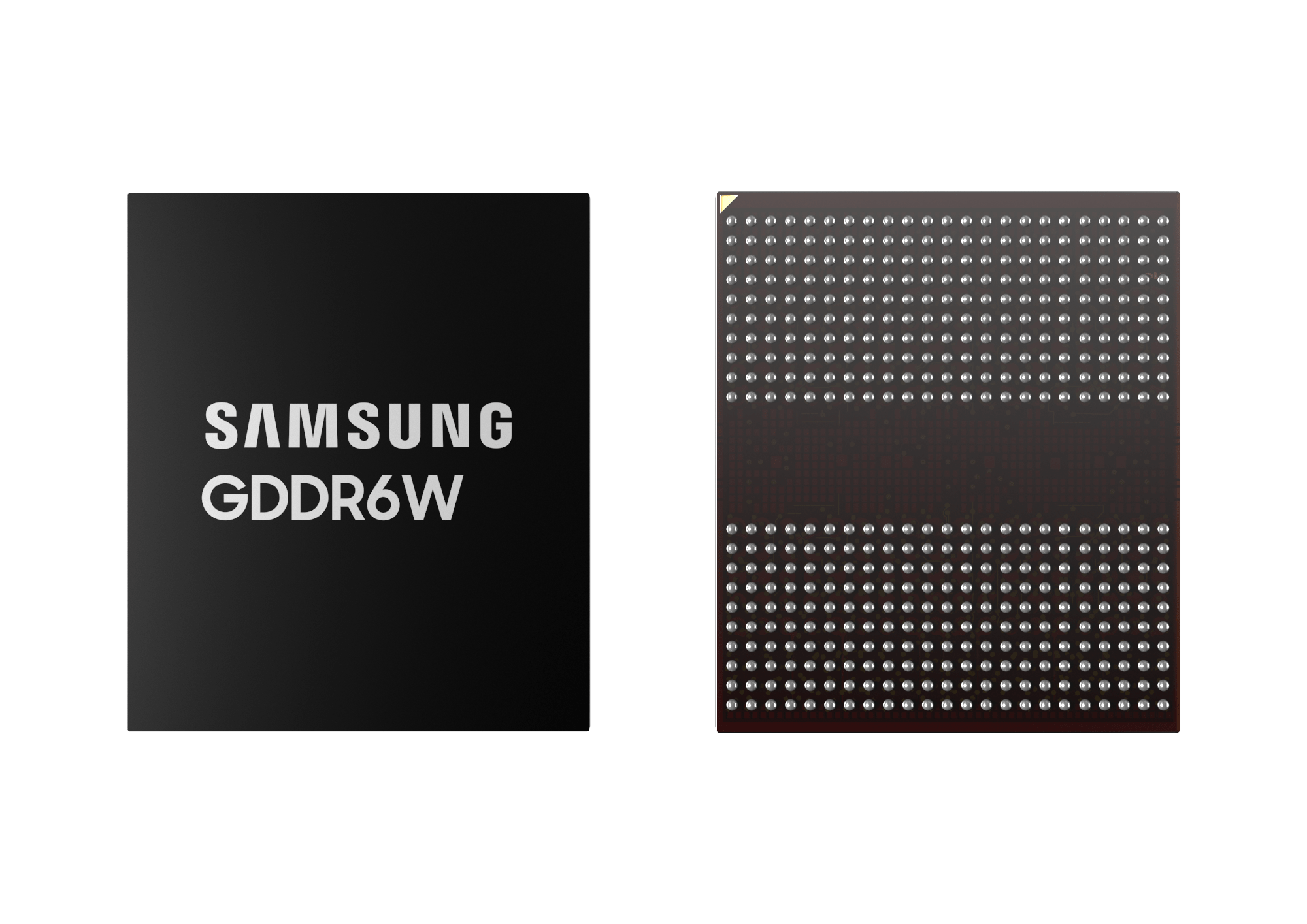
High performance, high capacity and high bandwidth memory solutions are helping bring the virtual realm to a closer match with reality. To meet this growing market demand, Samsung Electronics has developed GDDR6W (x64): the industry’s first next-generation graphics DRAM technology.
高性能、高容量和高带宽内存解决方案有助于使虚拟领域与现实更加匹配。为了满足这一不断增长的市场需求,三星电子开发了GDDR6W(x64):业界首个下一代图形DRAM技术。
GDDR6W builds on Samsung’s GDDR6 (x32) products by introducing a Fan-Out Wafer-Level Packaging (FOWLP) technology, drastically increasing memory bandwidth and capacity.
GDDR6W 以三星 GDDR6 (x32) 产品为基础,引入了扇出型晶圆级封装 (FOWLP) 技术,大幅增加了内存带宽和容量。
Since its launch, GDDR6 has already seen significant improvements. Last July, Samsung developed a 24Gbps GDDR6 memory, the industry’s fastest graphics DRAM. GDDR6W doubles that bandwidth (performance) and capacity while remaining the identical size of GDDR6. Thanks to the unchanged footprint, new memory chips can easily be put into the same production processes customers have used for GDDR6, with the use of the FOWLP construction and stacking technology, cutting manufacturing time and costs.
自推出以来,GDDR6已经有了重大改进。去年7月,三星开发了24Gbps GDDR6内存,这是业界最快的图形DRAM。GDDR6W 使带宽(性能)和容量翻倍,同时保持与 GDDR6 相同的大小。由于占地面积不变,新的存储芯片可以很容易地投入到客户用于GDDR6的相同生产工艺中,使用FOWLP结构和堆叠技术,从而减少制造时间和成本。
As shown in the picture below, since it can be equipped with twice as many memory chips in an identical size package, the graphic DRAM capacity has increased from 16Gb to 32Gb, while bandwidth and the number of I/Os has doubled from 32 to 64. In other words, the area required for memory has been reduced 50% compared to previous models.
如下图所示,由于它可以在相同尺寸的封装中配备两倍的内存芯片,因此图形DRAM容量从16Gb增加到32Gb,而带宽和I / O数量从32增加到64。换句话说,与以前的型号相比,内存所需的面积减少了 50%。

Generally, the size of a package increases as more chips are stacked. But there are physical factors that limit the maximum height of a package. What’s more, though stacking chips increases capacity, there is a trade-off in heat dissipation and performance. In order to overcome these trade-offs, we’ve applied our FOWLP technology to GDDR6W.
通常,封装的尺寸会随着更多芯片的堆叠而增加。但是有一些物理因素限制了包装的最大高度。更重要的是,虽然堆叠芯片增加了容量,但在散热和性能方面存在妥协。为了克服这些妥协,我们将FOWLP技术应用于GDDR6W。
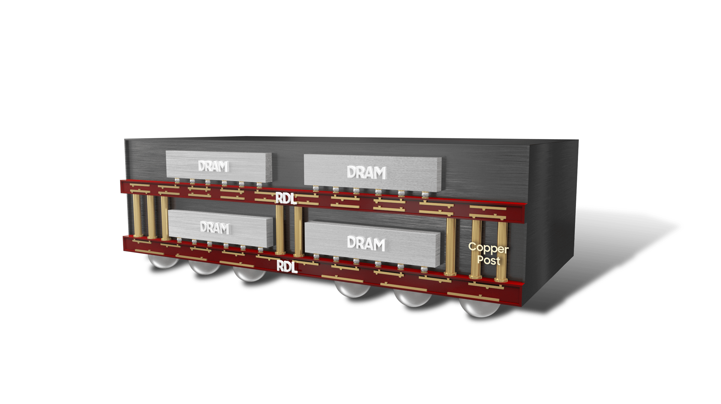
FOWLP technology directly mounts memory die on a silicon wafer, instead of a PCB. In doing so, RDL (Re-distribution layer) technology is applied, enabling much finer wiring patterns. Additionally, as there’s no PCB involved, it reduces the thickness of the package and improves heat dissipation.
FOWLP技术直接将存储芯片安装在硅晶圆上,而不是PCB上。在此过程中,应用了RDL(重布线层)技术,从而实现了更精细的布线模式。此外,由于不涉及PCB,因此减少了封装的厚度并改善了散热。
The height of the FOWLP-based GDDR6W is 0.7mm – 36% slimmer than the previous package with a height of 1.1mm. And despite the chip being multi-layered, it still offers the same thermal properties and performance as the existing GDDR6. Unlike GDDR6, however, the bandwidth of the FOWLP-based GDDR6W can be doubled thanks to the expanded I/O per single package.
基于 FOWLP 的 GDDR6W 的高度为 0.7 毫米,比之前的 1.1 毫米高度封装薄 36%。尽管该芯片是多层的,但它仍然提供与现有GDDR6相同的热性能和性能。然而,与GDDR6不同的是,基于FOWLP的GDDR6W的带宽可以翻倍,这要归功于每个封装的扩展I/O。
Packaging refers to the process of cutting fabricated wafers into semiconductor shapes or connecting wires. In the industry, this is known as a 'back-end process.' While the semiconductor industry has continuously developed towards scaling circuits as much as possible during the front-end process, packaging technology is becoming more and more important as the industry approaches the physical limits of chip sizes limits. That’s why Samsung is using its 3D IC package technology in GDDR6W, creating a single package by stacking a variety of chips in a wafer state. This is one of many innovations planned to make advanced packaging for GDDR6W faster and more efficient.
封装是指将制造的晶圆切割成半导体形状或连接线的过程。在行业中,这被称为“后端流程”。虽然半导体行业在前端工艺中不断朝着尽可能多地缩放电路的方向发展,但随着行业接近芯片尺寸限制的物理极限,封装技术变得越来越重要。这就是三星在GDDR6W中使用其3D IC封装技术的原因,通过在晶圆状态下堆叠各种芯片来创建单个封装。这是计划使GDDR6W先进封装更快、更高效的众多创新之一。
The newly developed GDDR6W technology can support HBM-level bandwidth at a system level. HBM2E has a system-level bandwidth of 1.6TB/s based on 4K system-level I/O and a 3.2Gpbs transmission rate per pin. GDDR6W, on the other hand, can produce a bandwidth of 1.4TB/s based on 512 system-level I/O and a transmission rate of 22Gpbs per pin. Furthermore, since GDDR6W reduces the number of I/O to about 1/8 compared with using HBM2E, it removes the necessity of using microbumps. That makes it more cost-effective without the need for an interposer layer.
新开发的GDDR6W技术可以在系统级别支持HBM级带宽。HBM2E 的系统级带宽为 1.6TB/s,基于 4K 系统级 I/O 和每引脚 3.2Gpbs 传输速率。另一方面,GDDR6W可以产生基于512个系统级I / O的1.4TB / s带宽和每个引脚22Gpbs的传输速率。此外,与使用 HBM2E 相比,GDDR6W 将 I/O 数量减少到约 1/8,因此无需使用微凸块。这使得它更具成本效益,而无需中介层。
| List | GDDR6W | HBM2E | | The number of System Level I/O | 512 | 4096 | | Pin Transmission Speed | 22Gbps | 3.2Gpbs | | System Level Bandwidth | 1.4TB/s | 1.6TB/s |
- System Level: Using graphics cards as an example, setting reference points of 8 package GDDR6W and 4 package HBM.
“By applying an advanced packaging technology to GDDR6, GDDR6W delivers twice the memory capacity and performance of similar-sized packages,” said CheolMin Park, Vice President of New Business Planning, Samsung Electronics Memory Business. "With GDDR6W, we’re able to foster differentiated memory products that can satisfy various customer needs – a major step towards securing our leadership in the market."
“通过将先进的封装技术应用于GDDR6,GDDR6W提供的内存容量和性能是类似尺寸封装的两倍,”三星电子内存业务新业务规划副总裁CheolMin Park说。“借助GDDR6W,我们能够培育出能够满足各种客户需求的差异化内存产品,这是确保我们在市场上的领导地位的重要一步。
Samsung Electronics completed the JEDEC standardization for GDDR6W products in the second quarter of this year. It has also announced that it will expand the application of GDDR6W to small form factor devices such as notebooks as well as new high-performance accelerators used for AI and HPC applications, through cooperation with its GPU partners.
三星电子在今年第二季度完成了GDDR6W产品的JEDEC标准化。它还宣布,将通过与GPU合作伙伴的合作,将GDDR6W的应用扩展到笔记本电脑等小型设备以及用于AI和HPC应用的新型高性能加速器。 |
 310112100042806
