本帖最后由 埃律西昂 于 2023-1-17 11:28 编辑
简介:
RISC-V世界中不仅有面向高能效小型内核的方向,也有数家企业在研发高性能大型内核。本帖带来分析师Dylan Patel对致力于此的Ventana Micro Systems的介绍。
相关链接: 《RISC-V阵营首款数据中心级CPU,最大128核的Ventana Veyron V1亮相》
来源:SemiAnalysis
原英文标题:《Ventana RISC-V CPUs Beating Next Generation Intel Sapphire Rapids!》
Ventana may be the most impressive due to the team, go-to-market strategy, and performance. They are also the closest to a commercial product. Ventana says their core is targeting everything from datacenter to automotive to 5G Edge to AI, and even client, but we believe the most advantageous value propositions will be in datacenters, networks, and 5G DU/RU, at least for the first generation.
由于团队、上市战略和绩效,Ventana 可能是最令人印象深刻的。它们也是最接近商业产品的。Ventana表示,他们的核心目标是从数据中心到汽车,从5G Edge到AI,甚至客户端,但我们相信最有利的价值主张将是数据中心,网络和5G DU / RU,至少对于第一代。
Ventana’s team has a long and storied history in the industry, including building the first 64-bit Arm core. Much of that team flowed through the progression of Veloce, Applied Micro, Macom, and Ampere Computing. Ventana has raised $108M total, with enough runway to get to their 2nd generation CPU.
Ventana的团队在业内有着悠久而传奇的历史,包括构建第一个64位Arm内核。该团队的大部分成员都经历了Veloce,Applied Micro,Macom和Ampere Computing的发展。Ventana总共筹集了1.08亿美元,有足够的跑道来获得他们的第二代CPU。
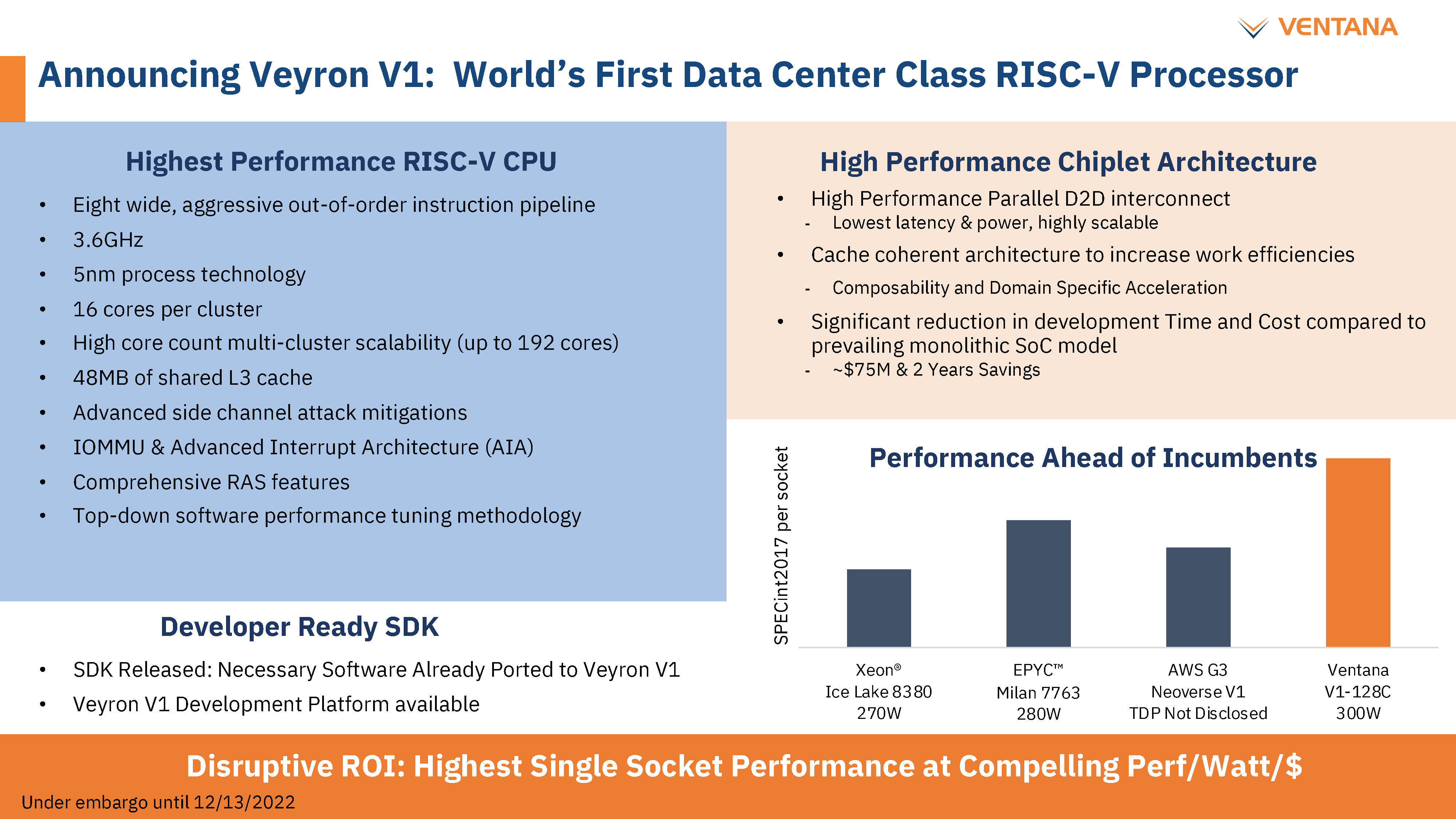
Cutting right to the chase, Ventana’s Veyron VT1 per core performance is comparable to the Neoverse V series from Arm (V1 in Amazon Graviton 3 and V2 in Nvidia Grace) but at higher clocks. Furthermore, it scales up to 128 cores within a 300W power budget. This is comparable performance to what AMD’s Genoa can do. Ventana can also achieve twice the core counts of Amazon’s Graviton 3, albeit with higher power.
切入正题,Ventana的Veyron VT1每核心性能可与Arm的Neoverse V系列(Amazon Graviton 3中的V1和Nvidia Grace中的V2)相媲美,但时钟更高。此外,它还可在 300W 功率预算内扩展到 128 个内核。这与AMD的热那亚可以做到的性能相当。Ventana还可以实现亚马逊Graviton 3核心数的两倍,尽管功率更高。
Another important distinction is that AMD Genoa and Graviton 3 are measured in silicon and available to customers. Ventana’s performance figures are a simulation with the actual tests coming after tape out in Q1. About new product introductions, we generally believe it’s all talk until the silicon is in the lab. Suppose these 1st party figures are missed by even 20%; Ventana will still smash Intel’s current generation Ice Lake and even Intel’s next-generation Sapphire Rapids, which doesn’t ship in high volume until mid-2023.
另一个重要的区别是AMD热那亚和Graviton 3是用硅测量的,可供客户使用。Ventana的性能数据是模拟的,实际测试是在第一季度流片后进行的。关于新产品的推出,我们通常认为在芯片进入实验室之前,一切都是空谈。假设这些第一方数字甚至错过了 20%,Ventana仍将粉碎英特尔当前一代的Ice Lake,甚至是英特尔的下一代蓝宝石急流,后者要到2023年中期才会大量出货。
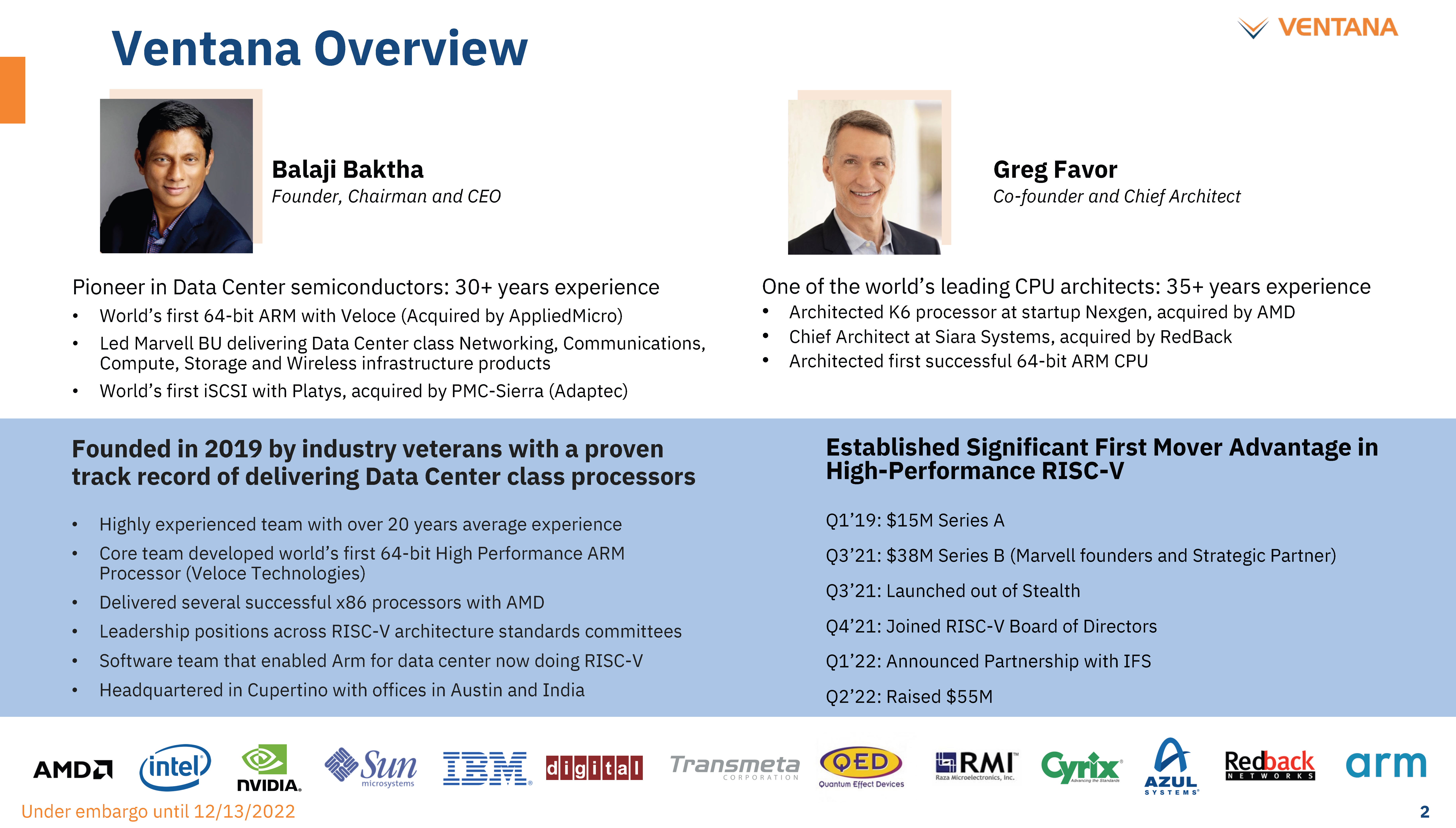
Before we go into technical details, we want to highlight the strength of the go-to-market strategy. Ventana isn’t only targeting the crowded bog-standard general-purpose CPU market. Ventana is making CPU chiplets that can be integrated into general-purpose CPU markets and various heterogeneous computing use cases. Furthermore, Ventana does not make the IO Die, but partners with firms on them. This unlocks a very different integration and partnership strategy. IO dies can either be taken off the shelf from existing providers or cheaply developed with mostly licensed IO and NOC IPs.
在讨论技术细节之前,我们想强调一下上市战略的优势。Ventana不仅针对拥挤的沼泽标准通用CPU市场。Ventana正在制造可以集成到通用CPU市场和各种异构计算用例中的CPU小芯片。此外,Ventana不会制造IO芯片,而是与相关公司合作。这开启了一个非常不同的整合和伙伴关系战略。IO芯片既可以从现有供应商那里购买,也可以使用大多数许可的IO和NOC IP廉价开发。
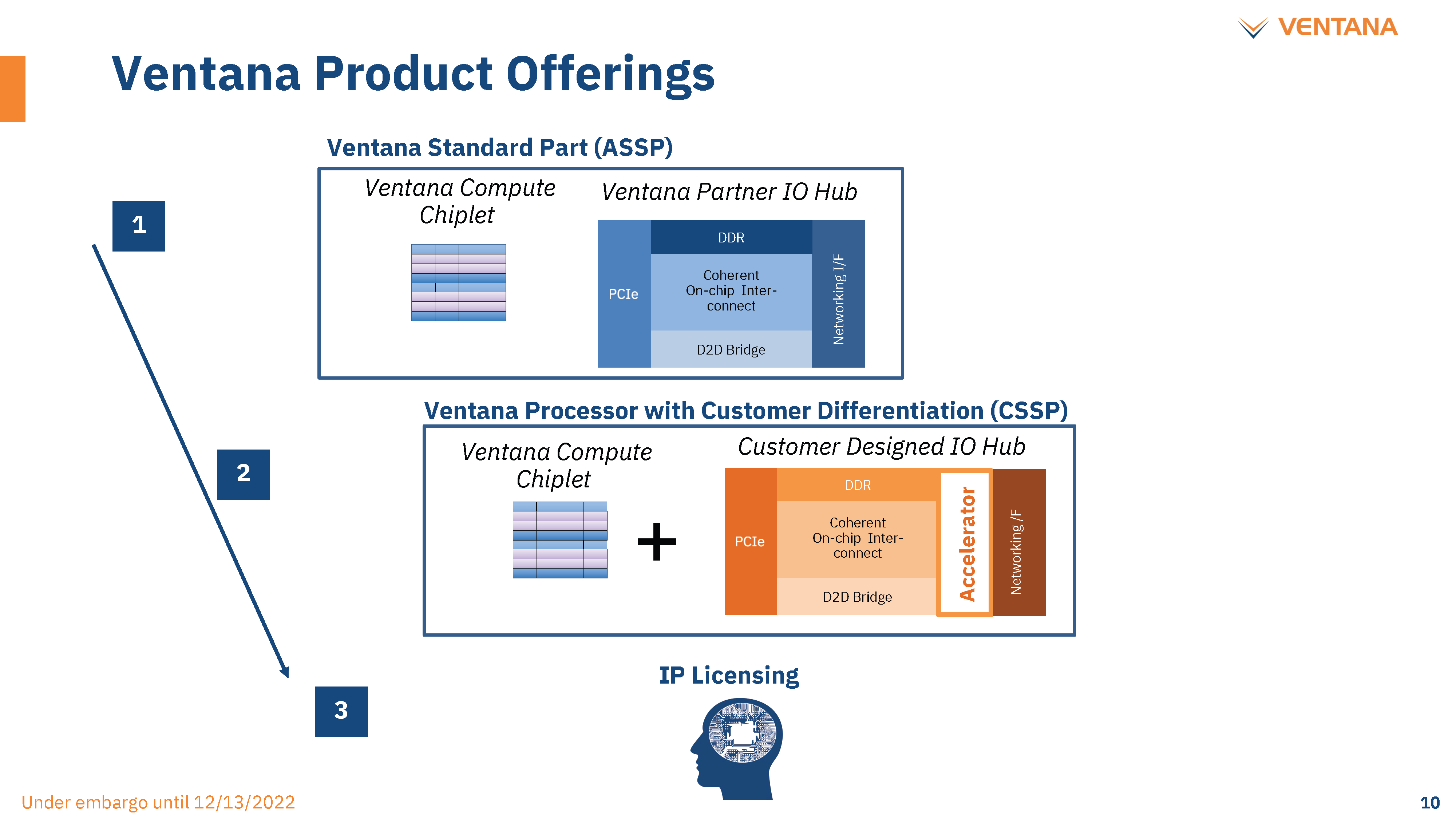
The customers can focus on their use cases and domain-specific accelerators. These domain-specific accelerators can be integrated directly on the IO die, and/or a chiplet can be developed. This strategy could work very well for the hyperscaler market as that is the exact business model they want.
客户可以专注于他们的用例和特定于域的加速器。这些特定于域的加速器可以直接集成在IO芯片上,和/或可以开发小芯片。这种策略对于超大规模市场非常有效,因为这正是他们想要的商业模式。
Companies like Amazon, Microsoft, Google, Meta, Alibaba, Tencent, and Baidu don’t like being at the whims of their suppliers who add more layers of margin stacking. Instead, they want to be in control and vertically integrate more of their offerings.
像亚马逊、微软、谷歌、Meta、阿里巴巴、腾讯和百度这样的公司不喜欢听从供应商的心血来潮,这些供应商增加了更多的利润堆叠层。相反,他们希望能够控制并垂直整合更多的产品。
There is no need for every hyperscaler and ASIC to reinvent the wheel. They can buy and integrate high-performance CPU chiplets at a much lower cost than fully packaged CPUs. Furthermore, when it comes to heterogenous compute and customized designs, the CPU chiplet design allows them to keep power and latency between the accelerators and the CPU minimal.
没有必要让每个超大规模企业和ASIC重新发明轮子。他们可以以比完全封装的CPU低得多的成本购买和集成高性能CPU小芯片。此外,当涉及到异构计算和定制设计时,CPU 小芯片设计允许他们将加速器和 CPU 之间的功耗和延迟保持在最低水平。
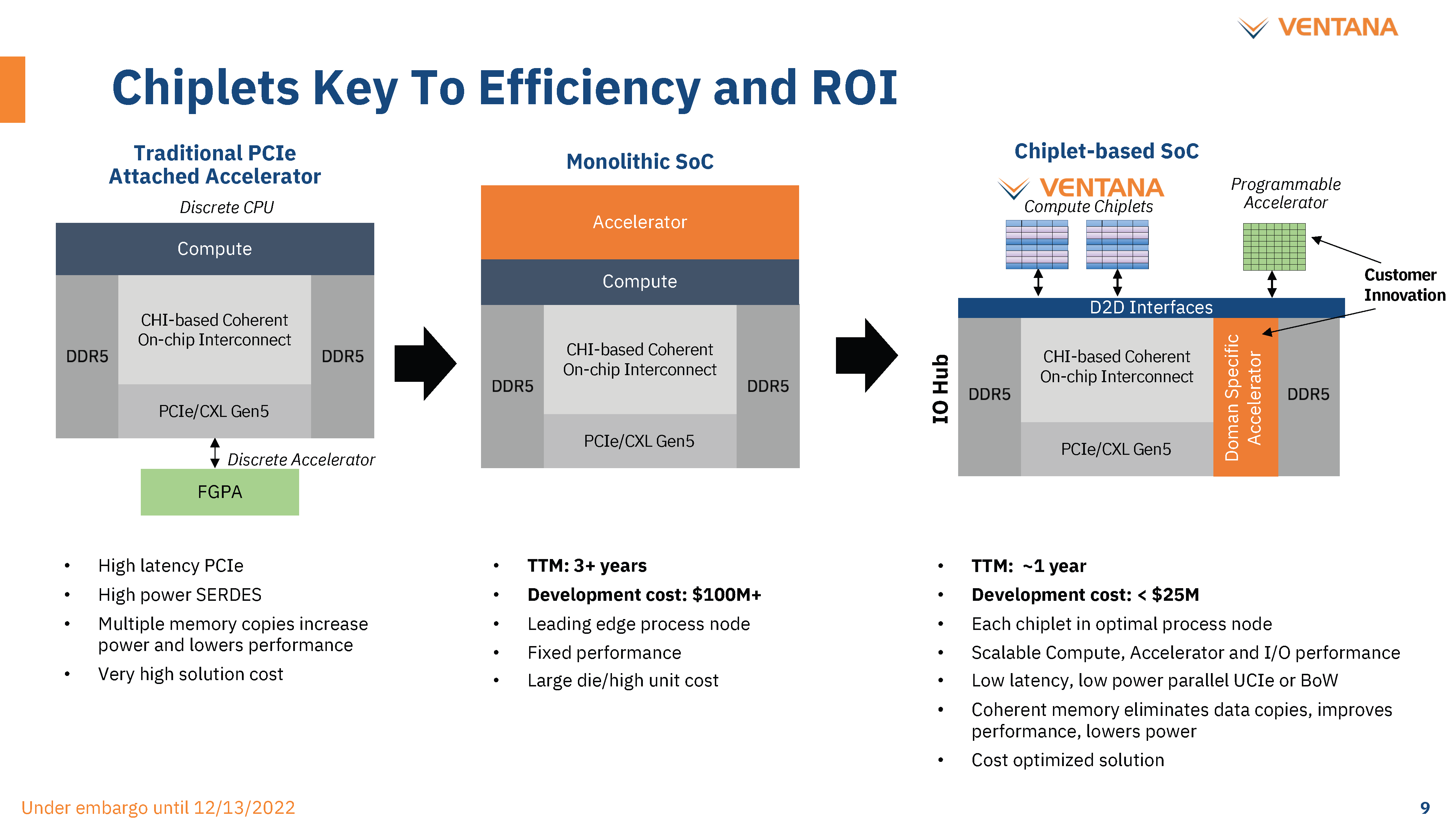
An IO die can be developed and taped out on TSMC’s 16nm for ~$20M. An IO Die on TSMC 7nm can be designed and taped out for ~$30M. This IO die can scale from a couple of memory controllers and a few PCIe ports to a massive amount of IO and networking. The incremental costs to create a new processor with the exact mix of high-performance CPU and dedicated ASICs integrated into the IO die or as a chiplet is relatively low, given the volumes of hyperscalers.
IO芯片可以在台积电的16nm上开发并流片,价格为~2000万美元。台积电 7nm 上的 IO 芯片可以设计和流片,价格为 ~3000 万美元。该 IO 芯片可以从几个内存控制器和几个 PCIe 端口扩展到大量的 IO 和网络。考虑到超大规模处理器的数量,创建新处理器的增量成本相对较低,该处理器将高性能CPU和专用ASIC精确地集成到IO芯片中或作为小芯片。
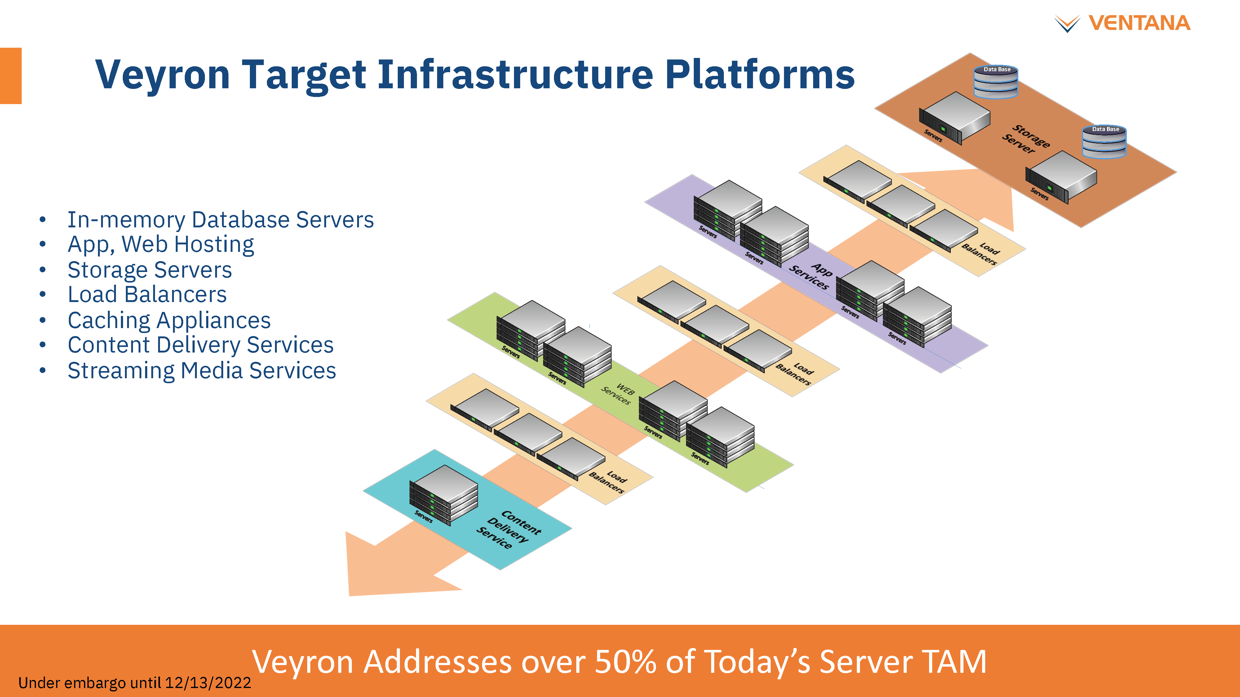
This business model can extend to the processors for 5G ORAN in the DU and RU, edge AI, edge gateway, in-memory databases, app/web hosting, storage servers, load balancers, caching appliances, content delivery networks, etc. As Moore’s Law crawls and workloads become more targeted by processors, the engineering costs for application-specific accelerators will soar unless an open chiplet approach is taken.
这种商业模式可以扩展到DU和RU中的5G ORAN处理器,边缘AI,边缘网关,内存数据库,应用程序/网络托管,存储服务器,负载平衡器,缓存设备,内容交付网络等。 随着摩尔定律缓慢爬行和工作负载越来越成为处理器的目标,除非采用开放式小芯片方法,否则特定应用加速器的工程成本将飙升。
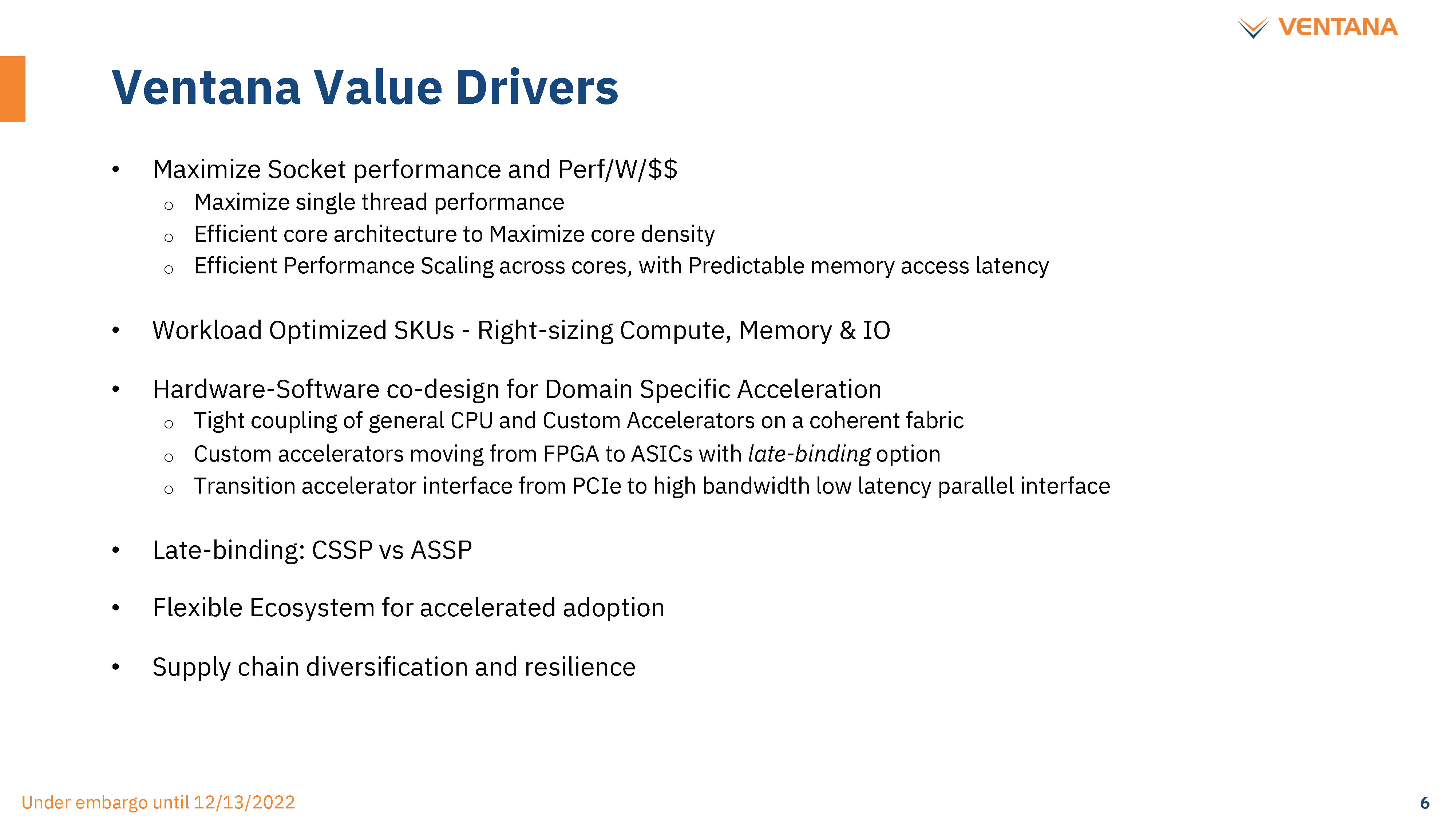

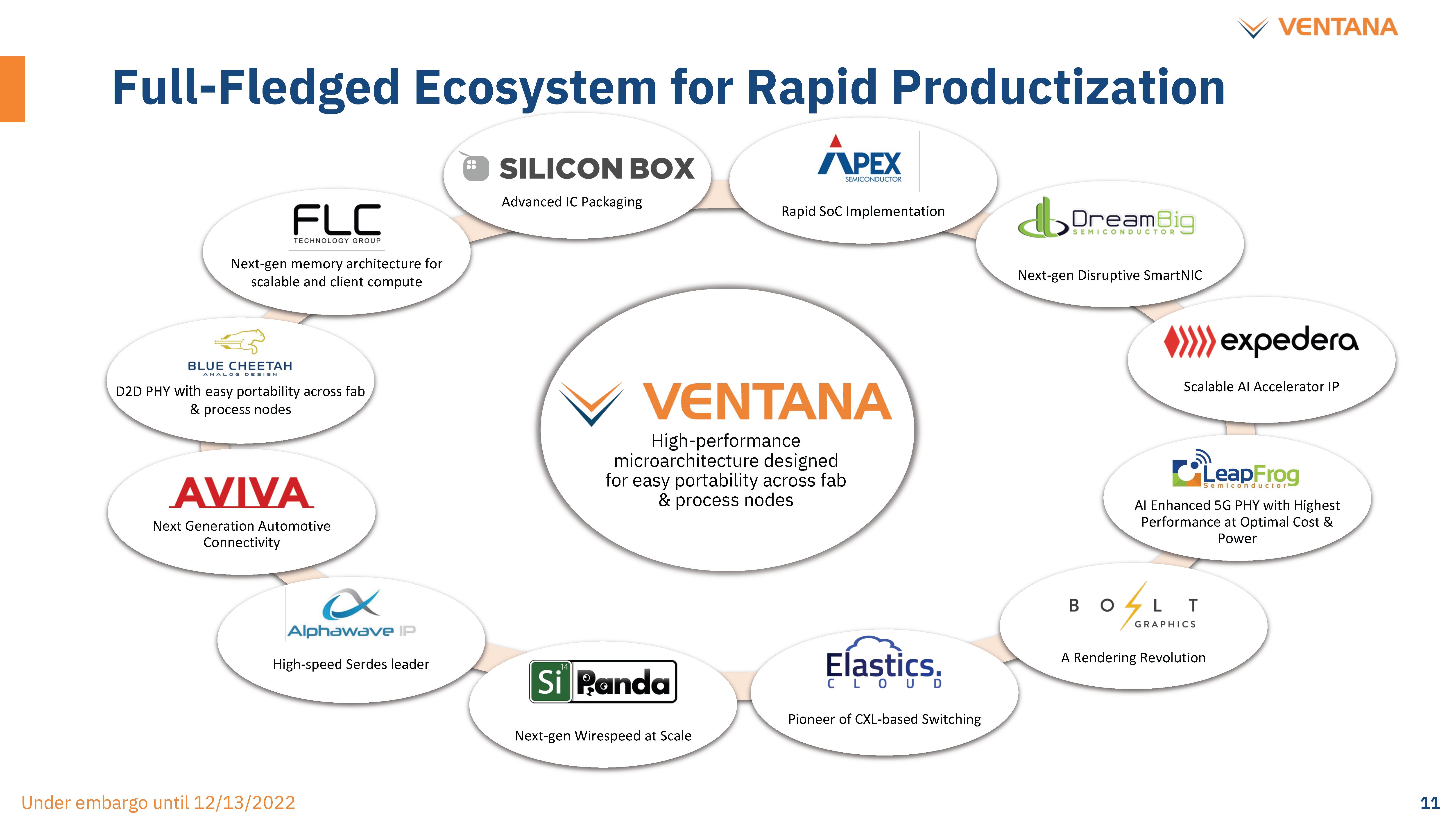
Ventana utilizes the Open Compute Project’s ODSA BOW standard for packaging. We know of at least 4 different compute-type chiplets and at least 3 different IO-related chiplets being made within this standard. While UCIe will be the winner in the long term, in 2023 and 2024, BOW will be more prevalent in the short term. Ventana is planning for future versions to support either BOW or UCIe. The chiplets / IO Die all uses the AMBA CHI protocol, which is much lower latency and power than CXL over UCIe.
Ventana利用OCP (Open Compute Project)的ODSA BOW标准进行打包。我们知道至少有 4 种不同的计算型小芯片和至少 3 种不同的 IO 相关小芯片正在此标准中制造。虽然UCIe将成为长期的赢家,但在2023年和2024年,BOW将在短期内更加普遍。Ventana正在计划未来的版本来支持BOW或UCIe。小芯片/IO芯片都使用AMBA CHI协议,该协议比基于UCIe的CXL低得多的延迟和功耗。
While AMD does have a chiplet CPU architecture and a custom silicon business, they do not utilize an open protocol. Furthermore, AMD is not willing to sell only CPU chiplets to hyperscalers. AMD wants to control the vertical stack from silicon design to packaging for any custom silicon deal. This strategy leads to more margin stacking and higher pricing. AMD’s choice makes sense for their business model but also leads to opportunities for hyperscalers to disaggregate them. Intel would follow the same lines as AMD for their business model, but their architecture won’t allow this level of disaggregation until 2025.
虽然AMD确实拥有小芯片CPU架构和定制芯片业务,但它们不使用开放协议。此外,AMD不愿意只向超大规模企业出售CPU小芯片。AMD 希望控制从硅设计到任何定制芯片交易的封装的垂直堆栈。这种策略会导致更多的利润堆叠和更高的定价。AMD的选择对他们的商业模式是有意义的,但也为超大规模企业带来了分解它们的机会。英特尔将遵循与AMD相同的商业模式,但他们的架构在2025年之前不允许这种级别的分解。
Ultimately, Ventana's strongest selling point is bringing the incremental cost of custom silicon to tens of millions of dollars from the current hundreds. When hyperscalers only buy some chiplets from fabless firms and the rest of their silicon directly from the foundries, the incremental cost per deployed package for a specific workload is significantly lower.
最终,Ventana最强大的卖点是将定制硅的增量成本从目前的数亿美元降低到数千万美元。当超大规模企业只从无晶圆厂公司购买一些小芯片,直接从代工厂购买其余芯片时,针对特定工作负载部署的每个封装的增量成本要低得多。
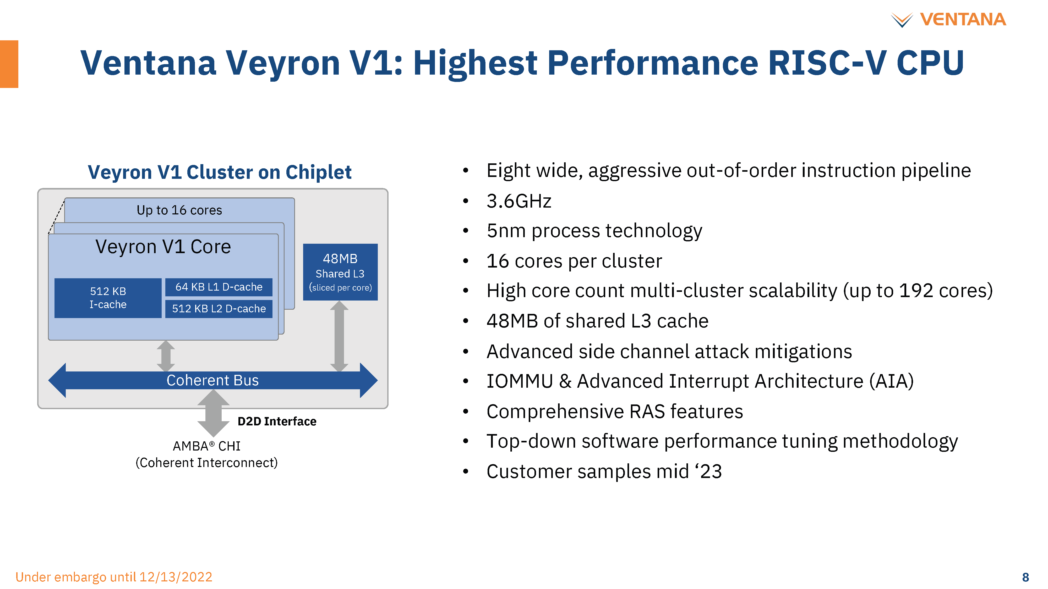
The core itself is pretty impressive. It is an 8 wide out-of-order core with a massive 512KB instruction cache. Each core comes with a 3MB L3 cache slice, although this is easily configurable in future versions. The goals with the core are quite simple but tough to achieve. Maximum single-threaded performance, maximum core density, efficient scaling across cores, and predictable/low latency across cores. It is noteworthy that VT1 does not have the RISC-V Vector extensions, as those were ratified too late into the design process. VT2, a relatively fast follow-on, will have the RISC-V Vector extensions.
核心本身令人印象深刻。它是一个 8 宽的无序内核,具有 512KB 的大量指令缓存。每个内核都带有一个 3MB L3 缓存片,尽管这在将来的版本中很容易配置。核心目标非常简单,但很难实现。最高的单线程性能、最大的内核密度、跨内核的高效扩展以及跨内核的可预测/低延迟。值得注意的是,VT1没有RISC-V矢量扩展,因为这些扩展在设计过程中批准得太晚了。VT2是一个相对快速的后续产品,将具有RISC-V矢量扩展。
The chiplet Ventana has developed scales up to 16 cores. One would think a chiplet with 16 big, high-performance CPU cores would result in a large die, but that’s perhaps the most impressive part about Ventana’s solution. The chiplet is 62mm^2 on TSMC’s N5 process technology. Compare that to AMD’s 8-core Zen 4 chiplet on N5, which is larger than Ventana’s 16-core chiplet.
Ventana小芯片已经开发出多达16个核心的规模。有人会认为具有16个大型高性能CPU内核的小芯片会产生一个大芯片,但这可能是Ventana解决方案中最令人印象深刻的部分。小芯片采用台积电N5工艺技术,尺寸为62mm²。相比之下,AMD在N5上的8核Zen 4小芯片比Ventana的16核小芯片大。
The economics are impressive. Ventana is also designing its CPU to make it easier to port across process nodes. For example, Ventana has a partnership with Intel’s IFS accelerator program, and we believe they will tape VT2 on Intel’s 3 or 18A process technology.
经济情况令人印象深刻。Ventana还在设计其CPU,使其更容易跨进程节点移植。例如,Ventana与英特尔的IFS加速器计划建立了合作伙伴关系,我们相信他们将在Intel 3或18A工艺技术上录制VT2。
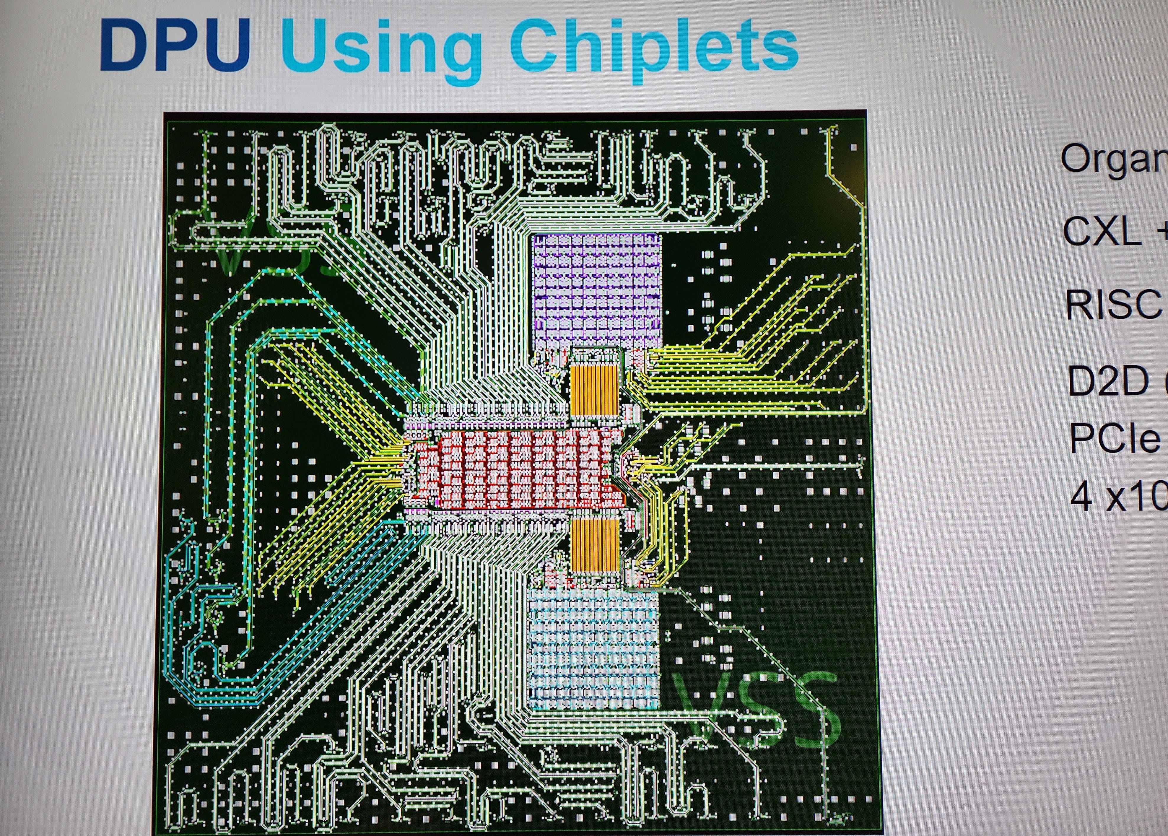
The picture above shows one of the multiple packages designed for Ventana VT1. This specific IO Die contains significant networking capabilities such as ethernet, packet processing, and CXL 2.0 into a DPU. Ventana uses BoW for their chip-to-chip interconnect with this IO Die with 1Tbps in each direction. That link has less than 2ns of latency from the PHY-to-PHY connection with <0.5pj/bit transferred between the IO die and CPU core chiplet.
上图显示了为Ventana VT1设计的多种封装之一。此特定 IO 芯片包含重要的网络功能,例如以太网、数据包处理和 DPU 中的 CXL 2.0。Ventana使用BoW与该IO芯片进行芯片到芯片互连,每个方向为1Tbps。该链路从 PHY 到 PHY 连接的延迟不到 2ns,IO 芯片和 CPU 内核小芯片之间传输的延迟为 <0.5pj/位。
Compared to Intel’s Sapphire Rapids, this is lower latency (<2ns vs. 2.4ns) and lower power (<0.5pj/bit vs. 0.5pj/bit), and compared to AMD’s Zen 4, this is lower latency and much lower power (<0.5pj/bit vs. <2pj/bit). The Ventana chiplet package is a standard 8-2-8 organic substrate with 130um microbumps, whereas Intel had to use their more costly EMIB advanced packaging with 55um microbumps to achieve those results.
与英特尔的Sapphire Rapids相比,这是更低的延迟(<2ns对2.4ns)和更低的功耗(<0.5pj /位对0.5pj /bit),与AMD的Zen 4相比,这是更低的延迟和更低的功耗(<0.5pj /位vs. <2pj/bit)。Ventana 小芯片封装是具有 130um 微凸块的标准 8-2-8 有机基板,而英特尔必须使用具有 55um 微凸块的更昂贵的 EMIB 高级封装来实现这些结果。

With the right go-to-market strategy and impressive performance, Ventana could be successful, but the software story is also a big part of the conversation. It took Arm a decade from announcing their push into server to getting deployed en mass. RISC-V will take a lot less time because the systems and software are more equipped to switch, but it is a big concern. Ventana knows this just as well as anyone else, where many members of the team experience exactly these teething pains as the first 64-bit Arm core and through their legacy to Ampere Computing.
凭借正确的上市策略和令人印象深刻的性能,Ventana可能会成功,但软件故事也是对话的重要组成部分。Arm 从宣布进入服务器到大规模部署花了十年时间。RISC-V将花费更少的时间,因为系统和软件更有能力进行切换,但这是一个大问题。Ventana和其他任何人都一样了解这一点,团队中的许多成员正是在第一个64位Arm内核以及他们给Ampere Computing的遗产中经历了这些初期的痛苦。
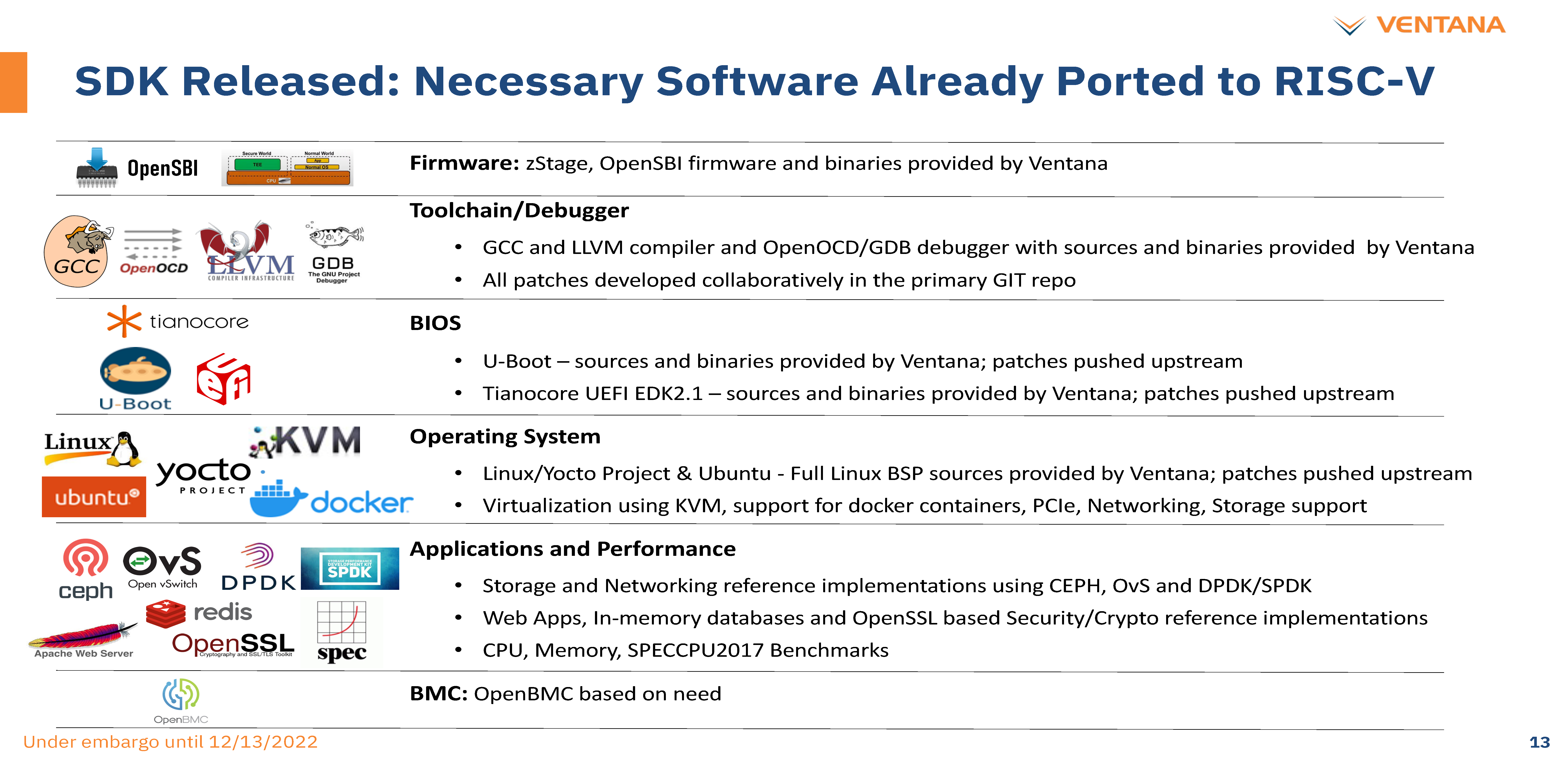
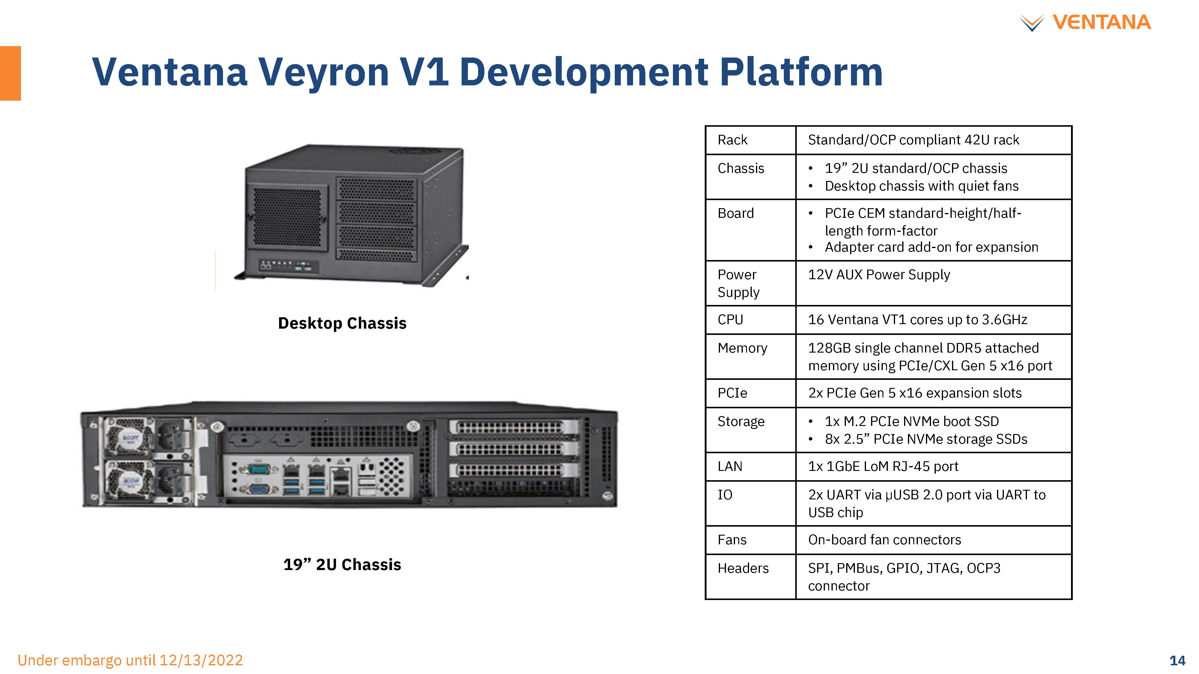
Ventana claims to have a ton of software for many applications ready, especially on the low-level, storage, and networking applications. Ventana has been able to work on software without its own silicon by using SiFive-based development boards, which have ISA compatibility. In that sense, the challenge of bringing the server software ecosystem to RISC-V started 3 years ago. If Arm took 10 years, and RISC-V is on an accelerated timeline that will take half the time, then potentially, we are only a couple of years away from RISC-V in the datacenter.
Ventana声称为许多应用程序准备了大量软件,尤其是在低级,存储和网络应用程序上。Ventana通过使用具有ISA兼容性的基于SiFive的开发板,能够在没有自己芯片的软件上工作。从这个意义上说,将服务器软件生态系统引入RISC-V的挑战始于3年前。如果Arm花了10年时间,而RISC-V的加速时间线将花费一半的时间,那么在数据中心,我们可能距离RISC-V只有几年的时间。
That’s the optimistic view, of course. We expect 5G ORAN, networking, and hyperscale internal workloads to be able to jump potentially sooner, but general-purpose multi-tenant cloud instances are much, much further away. The development kit with Ventana’s CPU chiplet will be available in the middle of next year, with volume shipments late next year.
当然,这是乐观的看法。我们预计5G ORAN、网络和超大规模内部工作负载可能能够更快地跳跃,但通用多租户云实例要远得多。带有Ventana的CPU小芯片的开发套件将于明年年中上市,明年年底将批量出货。 |
 310112100042806
